- Separate filling defects from release, curing, contamination, and alignment defects before changing the formulation.
- Measure residual-layer uniformity and optical loss, not only visual appearance.
- Control surface preparation, adhesive viscosity, dispense volume, temperature, pressure, and cure exposure as one process window.
- Use witness structures and defect maps to connect local defects with wafer-scale process conditions.
- Escalate to a custom nanoimprint adhesive when the required refractive index, shrinkage, release behavior, or optical durability cannot be achieved with a standard material.
Nanoimprint adhesive selection directly affects optical device yield because the adhesive must fill nanoscale relief, cure with limited shrinkage, release without damaging the mold, and maintain optical performance after aging. Research reviews such as the Nature Materials review of nanoimprint lithography identify pattern transfer, materials behavior, and defect control as connected process challenges rather than isolated formulation issues.
Why nanoimprint adhesive defects are difficult to diagnose
The first diagnostic conclusion should be based on where the defect appears in the process sequence.
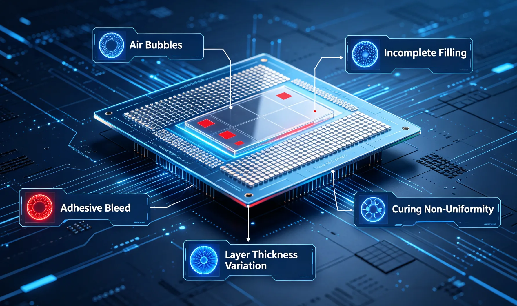
In an optical device line, the same visible symptom can have different causes. A missing diffractive feature may result from insufficient filling, trapped gas, contamination on the template, inadequate adhesion to the substrate, or a release event that tears the cured material away. A haze defect may come from particles, phase separation, incomplete conversion, or a refractive-index mismatch at an interface.
That is why yield improvement begins with a defect map containing location, morphology, orientation, affected area, cure condition, mold history, and inspection method. A defect that repeats at the same radial position suggests a tool, chuck, coating, or dispense issue. A random defect distribution more often points toward particles, bubbles, handling, or uncontrolled material aging.
| Diagnostic stage | Primary question | Useful observation | Process action |
|---|---|---|---|
| 1 | Did the liquid reach the full pattern area? | Unfilled corners or dry islands | Review viscosity, dispense layout, temperature, and imprint pressure |
| 2 | Was gas displaced? | Round voids or repeated bubble clusters | Review dispense sequence, surface wetting, and ambient control |
| 3 | Did the material cure uniformly? | Local haze, tack, or dimensional variation | Review exposure dose, optical transmission, and cure depth |
| 4 | Did the cured layer release cleanly? | Torn features, residue, or mold sticking | Review release treatment, adhesion balance, and demolding speed |
| 5 | Did the optical interface remain stable? | Scattering, color shift, or drift after aging | Review refractive index, moisture uptake, contamination, and thermal history |
Problem 1: Incomplete filling and missing optical features
Incomplete filling is usually a wetting and flow problem before it is a pressure problem.
For diffractive optical elements, waveguides, and microstructured optical films, the adhesive must enter narrow cavities without leaving voids or height loss. Excessive viscosity, poor substrate wetting, insufficient liquid volume, premature skin formation, and an unfavorable dispense pattern can all produce incomplete transfer.
A common mistake is increasing pressure immediately. Higher pressure may close some shallow gaps while worsening particle-induced damage, increasing tool stress, or pushing material away from the active area. A better sequence is to verify surface cleanliness, compare contact behavior on the actual substrate, and then adjust temperature, dispense distribution, and imprint time.
Practical corrective actions
- Measure viscosity at the actual process temperature rather than relying only on a room-temperature specification.
- Compare center, edge, and corner fill using cross-sections or high-resolution optical inspection.
- Check whether the liquid volume is sufficient for the patterned area and expected residual layer.
- Use a staged experiment that changes one factor at a time: wetting, temperature, dispense pattern, then pressure.
Optical yield is especially sensitive when a small missing region interrupts a waveguide path or changes the duty cycle of a diffraction grating. The right acceptance criterion should therefore combine pattern completeness with optical performance, not treat them as separate quality gates.
Problem 2: Bubbles, voids, and trapped air
Trapped air is commonly created when the adhesive advances around a feature or particle faster than gas can escape.
Bubbles may originate in the liquid, the syringe, the dispense tip, the substrate texture, or the mold contact sequence. They can also appear when a liquid contains dissolved gas that comes out of solution during temperature or pressure changes. In optical devices, even a small void can scatter light, interrupt coupling, or create a local thickness change.
Bubble diagnosis should compare the defect shape with the flow direction. Rounded voids inside otherwise complete areas suggest gas entrapment. Long channels or wedge-shaped empty zones are more consistent with nonuniform contact or a flow front that has been blocked. Repeated bubble locations may indicate a dispense nozzle or mold feature rather than random contamination.
| Bubble evidence | Likely source | Severity score | Recommended first check |
|---|---|---|---|
| Isolated circular void | Liquid or dispense gas | 1 | Degassing and dispense handling |
| Repeated void line | Flow-front obstruction | 2 | Surface wetting and contact sequence |
| Edge-only voids | Insufficient edge coverage | 3 | Dispense volume and edge geometry |
| Void clusters near particles | Contamination or roughness | 4 | Particle control and substrate inspection |
| Large-area delamination void | Adhesion or cure failure | 5 | Surface treatment and cure verification |
The severity score above is a practical troubleshooting scale, not a published industry benchmark. It helps production teams prioritize defects that affect active optical area, repeat across panels, or trigger downstream delamination.
Problem 3: Residual-layer nonuniformity
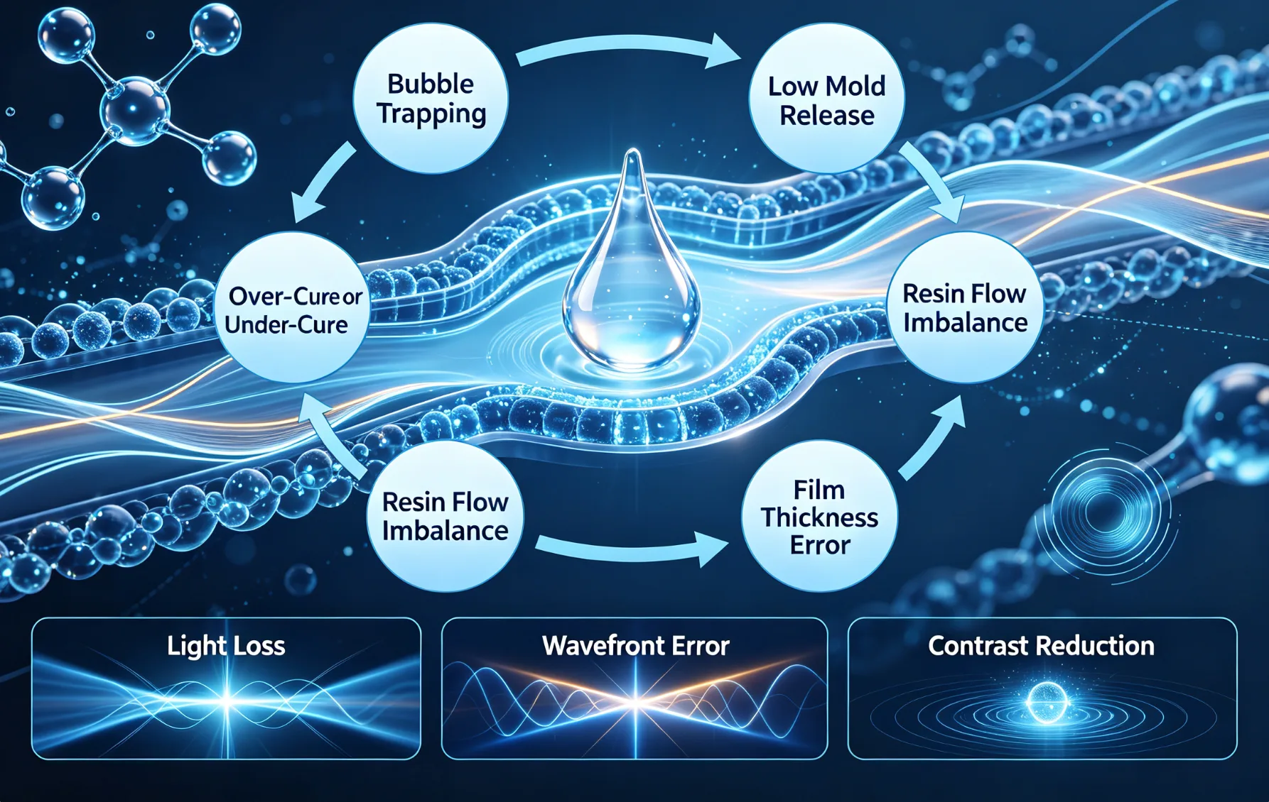
Residual-layer variation can convert an apparently successful imprint into an optical performance failure.
After imprinting, the material left between the substrate and the lowest patterned regions may vary across the device. Causes include nonuniform liquid distribution, substrate bow, mold tilt, pressure gradients, local temperature differences, and changes in adhesive volume. In a subsequent etch or transfer step, this variation can produce different etch times across the wafer or panel. In a direct optical stack, it can change phase delay, coupling efficiency, or interface thickness.
Do not judge residual-layer quality from a single center measurement. Map the active area using a repeatable measurement method and compare thickness with optical output. If residual-layer variation follows the chuck or mold orientation, investigate mechanical flatness and alignment. If it follows dispense position, investigate volume distribution and flow.
A robust control plan records the residual-layer map together with adhesive batch, age, temperature, substrate lot, mold clean count, cure condition, and demolding result. This history allows engineers to distinguish formulation drift from equipment drift.
Problem 4: Adhesive sticking, residue, and demolding damage
Release failure occurs when adhesion to the mold is stronger than the mechanical integrity of the cured optical layer.
Sticking can leave residue on the template, tear high-aspect-ratio features, round sharp corners, or transfer particles into the next imprint. The failure is often described as a release problem, but the root cause may be an adhesion imbalance between mold, adhesive, and substrate. Excessive cure shrinkage can increase interfacial stress. Incomplete cure can leave the layer soft and tacky. Overly aggressive release treatment can reduce mold adhesion but weaken bonding to the substrate.
Demolding speed and direction also matter. A sudden peel force can damage structures that survive a slower, more controlled separation. The safest approach is to optimize release chemistry and cure behavior together while monitoring both mold residue and substrate-side delamination.
Release troubleshooting checklist
- Inspect the mold before and after imprinting for residue, scratches, and localized contamination.
- Compare fresh and repeatedly used mold conditions to identify release-treatment depletion.
- Check cure completeness at the actual optical stack thickness, not only in a thick laboratory film.
- Measure substrate adhesion after cure and after the intended thermal or humidity exposure.
- Review demolding force, speed, angle, and temperature as controlled process variables.
For optical manufacturing, a material that releases easily but bonds poorly is not a successful solution. The target is a balanced interface that supports clean demolding, stable optical geometry, and long-term adhesion.
Problem 5: Cure variation, optical haze, and refractive-index drift
Cure inconsistency can reduce yield even when pattern transfer looks acceptable.
Optical adhesives often contain multifunctional monomers, photoinitiators, additives, and high-refractive-index components. Their final behavior depends on exposure uniformity, film thickness, oxygen inhibition, temperature, spectral transmission through the stack, and post-cure history. Local under-cure can cause tack, migration, haze, or aging drift. Excessive cure or rapid polymerization can increase shrinkage stress and distort the structure.
Optical haze should be investigated through both imaging and material analysis. A cloudy region may be caused by microbubbles, phase separation, surface roughness, contamination, or refractive-index variation. These mechanisms require different corrective actions, so increasing exposure is not a universal answer.
The National Institute of Standards and Technology overview of nanotechnology provides useful context for why nanoscale material behavior, measurement, and process control are important in advanced manufacturing. For a production line, the practical implication is clear: define cure and optical acceptance using measurable outputs such as transmission, haze, feature fidelity, adhesion, and aging stability.
| Observed condition | Possible mechanism | Optical risk | Priority test |
|---|---|---|---|
| Clear but tacky surface | Incomplete conversion or oxygen inhibition | Contamination and layer movement | Surface cure and solvent-resistance check |
| Uniform milky appearance | Phase separation or index mismatch | Scattering and coupling loss | Microscopy and transmission measurement |
| Localized cloudy patches | Bubbles, particles, or exposure nonuniformity | Local optical loss | Defect map correlated with exposure field |
| Feature distortion after cure | Shrinkage stress or adhesion imbalance | Phase and dimensional error | Before-and-after profile measurement |
How to build a yield-focused adhesive process window
A useful process window links material properties to measurable device outcomes.
Start with a controlled matrix covering viscosity, substrate temperature, dispense volume, imprint time, pressure, cure exposure, and demolding conditions. The exact settings should be established on the production tool because mold geometry, optical stack, lamp spectrum, and mechanical behavior can change the result.
Use three layers of evidence: material data, process data, and device data. Material data include viscosity stability, refractive index, cure response, shrinkage, adhesion, and storage behavior. Process data include fill time, defect density, residual-layer map, mold residue, and demolding force. Device data include transmission, haze, diffraction efficiency, coupling performance, and aging results.
Supplier collaboration becomes valuable when the problem involves several variables at once. A custom formulation may be justified when the device requires a narrow refractive-index match, low optical absorption, specific release behavior, low shrinkage, or compatibility with a sensitive substrate. The supplier should provide not only a liquid but also application guidance, batch consistency information, and a clear boundary between demonstrated performance and development targets.
When to change the nanoimprint adhesive
Change the adhesive only after confirming that cleaning, dispense, tooling, cure, and measurement systems are not masking the real cause.
A formulation change is reasonable when defects remain after the process is stabilized and the material cannot meet the required combination of wetting, flow, optical clarity, refractive index, cure response, adhesion, release, and environmental stability. Changing materials without preserving a controlled baseline makes it difficult to know whether yield improved because of chemistry or because of uncontrolled process variation.
For optical manufacturers, the best development brief describes the substrate, mold material, feature geometry, target optical function, cure method, expected operating environment, inspection method, and known failure modes. This allows material developers to optimize molecular design and formulation around the device rather than around a single laboratory test.
FAQ
What is the most common nanoimprint adhesive defect?
Incomplete filling and trapped air are common early-stage defects, but the dominant issue depends on mold geometry, surface treatment, dispense method, and cure process. A defect map is more reliable than assuming one universal root cause.
Can higher imprint pressure eliminate adhesive defects?
Not reliably. Higher pressure may improve contact in some cases, but it can also increase tool stress, move the liquid out of the active area, or worsen particle damage. Wetting, viscosity, dispense distribution, and pressure should be optimized together.
How do bubbles affect optical device yield?
Bubbles can scatter light, interrupt a waveguide path, change local thickness, and create sites for delamination. Their effect depends on size, location, and whether the void intersects the active optical structure.
Why is residual-layer uniformity important?
Residual-layer variation changes the optical interface and can also create nonuniformity in downstream etching or pattern transfer. Mapping the layer across the complete active area is more informative than checking one point.
What causes adhesive sticking during demolding?
Typical causes include inadequate mold release treatment, excessive mold adhesion, incomplete cure, high cure stress, contamination, and weak substrate bonding. Demolding force and residue inspection help separate these mechanisms.
Should optical adhesives be selected by refractive index alone?
No. Refractive index must be considered with absorption, haze, viscosity, cure shrinkage, adhesion, release, thermal behavior, moisture resistance, and compatibility with the optical stack. A high index that creates haze or poor durability may reduce total device yield.
When should a manufacturer request a custom adhesive?
Custom development is appropriate when standard materials cannot meet the required optical index, flow behavior, cure method, release balance, substrate adhesion, or environmental stability within a repeatable production window.
About the materials partner
Merak develops optical functional materials for micro-nano optics, optical communications, coatings, display modules, and eyewear surface treatment. Its capabilities span molecular design, synthesis, formulation development, refractive-index control, and application support. This model is relevant to manufacturers that need more than a catalog liquid and require material optimization, batch consistency, and process introduction assistance. Contact the technical team to discuss an optical adhesive or interface-material requirement.